On behalf of the RADECS 2024 organizing committee, we extend a warm welcome to all participants in this exciting thematic workshop!
This workshop dives deep into the ever-evolving world of Single Event Effect (SEE) testing, exploring both established and emerging methodologies.
This one-day event is divided into two distinct sessions:
- Morning Session: We’ll begin by delving into the well-defined practices of conventional radiation effects testing methodologies. This session will provide a solid foundation for understanding the current standards and best practices in SEE testing using heavy-ion, proton and neutron beams.
- Afternoon Session: The afternoon takes us on a journey into the future. We’ll explore innovative approaches pushing the boundaries of SEE testing. This session will cover advancements ranging from laser and synchrotron x-ray testing to the applications of very high energy ion beams, and system level testing. We’ll conclude by exploring the unique radiation challenges faced by quantum computing and how these challenges might impact its development.
Both sessions will be followed by 40-minute panel discussions. This offers a unique opportunity to engage with leading experts, share knowledge, and foster discussions on the critical role of SEE testing in ensuring the reliability of electronics in harsh radiation environments.
Furthermore, we will encourage active participation throughout the day. Don’t hesitate to ask questions, share your experiences, and engage in thought-provoking discussions with your fellow attendees and speakers.
Let’s embark on this exploration of the present and future of SEE testing together!
Program
| Morning Session: Conventional Testing | |||
| 09:00 | 20m | Introduction | Arto Javanainen Gerd Datzmann |
| 09:20 | 30m | Evolution of SEE Testing over the Years | Dolores A. Black |
| 09:50 | 30m | Best Practices for SEE Testing – Heavy Ions and Protons | Gregory R. Allen |
| 10:20 | 30m | Best Practices for SEE Testing – Neutrons | Cécile Weulersse Maria Mazurek |
| 10:50 | 30m | Coffee Break | |
| 11:20 | 30m | Developing Neutron Testing Capacity & Capability in Europe | Christopher D. Frost |
| 11:50 | 30m | RADNEXT Unveiled: A Full Overview on the First Distributed Research Infrastructure Worldwide for the Radiation Hardness Testing of Microelectronic Devices | Jochen Kuhnhenn Ennio Capria |
| 12:20 | 40m | Panel Discussion | |
| 13:00 | 90m | Lunch | |
| Afternoon Session: Alternative Approaches | |||
| 14:30 | 5m | Introduction | Arto Javanainen |
| 14:35 | 25m | SEE Testing with Laser | Thomas Borel |
| 15:00 | 25m | SEE Testing with Pulsed X-rays: Perspectives and Current Status | Françoise Bezerra |
| 15:25 | 25m | High Energy Heavy Ions (>100 MeV/n) | Kevin A. Brown |
| 15:50 | 25m | Radiation Qualification at CERN: From Components to System Level Using COTS | Salvatore Danzeca |
| 16:15 | 30m | Coffee Break | |
| 16:45 | 25m | Impact of Ionizing Radiation on Quantum Processors | Antti Vepsäläinen |
| 17:10 | 40m | Panel Discussion | |
| 17:50 | 10m | Closing of the Workshop | |
Speakers & Talks
Morning Session: Conventional Testing
Evolution of SEE Testing over the Years
Abstract
The evolution of SEE testing over the years can be tied directly to the evolution of the microelectronics fabrication. Fabrication technology has scaled down in size over the years to increasing the number of transistors per IC, increasing the frequency at which they can operate, and reducing power and costs to end users. In order to yield low-cost ICs as the technology scaled, fabs increased the number of metal routing layers, added redundant transistors/logic cells, and integrated multiple different types of circuits onto the same IC (SoC). All of these lead to an increased complexity of SEE testing. Topics to be included in this talk include:
- Increase in Metal layer and decrease in transistor size leads to challenges for angled SEE testing.
- Unknown redundant circuits can impact observed results.
- Many different circuit types, ie, memory, processor, etc., on the same IC make it difficult to determine the root of SEEs and may impact the observability of SEEs.
- Operating a high speed IC at its normal frequency may not be feasible in SEE testing.
- The tight spacing of transistors make multiple node charge collection more likely.
- The hardened by design techniques for mitigating SEEs require particles that are near impossible to generate in ground based facilities.
The ultimate goal of SEE testing is to determine the effect rates at the most basic circuit elements. Rate prediction of the IC is based upon those rates with considerations for their relative usage in the application. The ability to observe and count effects in basic circuit elements will continue to create interesting challenges for SEE testing.
Biography
Dolores Black currently works at Sandia National Laboratories, in the Radiation Research Group. She started her career as a circuit designer for analog, digital, mixed-signal board design and PLD, FPGA and SoC for military and space applications while working at Honeywell and Xilinx. She received her PhD in Single Event Transient faults for complex ICs, from radiation transport to full circuit simulation, validating results through experimentation. At Sandia, she currently works in both the experimental and mod/sim for SEEs and Dose Rate.
Abstract
There is no one right approach to plan and execute a single event effects (SEE) test. There certainly are numerous ways to improve efficiency, correctness, and success of an SEE test. The SEE test needs of the radiation effects community are as diverse as the electronics we test, and as such results in a sundry solution space for approaching test campaigns. This talk will provide attendees with a generalized approach that will serve to support testers whether from academia, research, industry, or civil and defense sectors. Touching on topics ranging from facility selection, to test planning, execution, and reporting, attendees will walk away with an improved likelihood of SEE test success.
Biography
Gregory Allen has spent the last 20 years working in the radiation effects field, focusing on single event effects accelerators, spending most of his time in accelerators testing electronics for use in the natural space environment. Greg received a B.S. in Computer Engineering from CSU, Chico and an M.S. in System Architecting and Engineering from the University of Southern California. Greg is a senior radiation effects engineer at the Jet Propulsion Laboratory, California Institute of Technology. Greg is the co-lead for the Jet Propulsion Laboratory's Center for Space Radiation and Group Lead for the Radiation Effects Group.

Abstract
Shrinking feature sizes in electronic systems and increasing their complexity have led to a growing Single Event Effects (SEE) susceptibility arising from cosmic rays, either at aircraft altitudes or at seal level. To ensure a system meets all its safety and reliability requirements, neutron induced failures need to be considered, including testing of the components or systems in a neutron beam, in order to evaluate the expected error rate of the final application.
This short course will focus on how to establish the SEE sensitivity towards the neutron part of the terrestrial environment. It will cover accelerated soft error rate test facilities and methods. Some guidelines will be provided to obtain valuable neutron cross-sections and associated uncertainties.
Biography
Cécile Weulersse has worked for 20 years at Airbus, accumulating a broad experience on SEE predictive tools and SEE test methodologies for the needs of the aerospace divisions. In 2021, she joined a research team on electrification technologies. Her new research interests include superconductivity, energy storage and power electronics.
Maria Mazurek received her Master's and Engineer degrees in microelectronics from Telecom Bretagne Brest (France) and from Gdansk University of Technology (Poland) in 2009. From 2009 to 2013, she was with HIREX Engineering, France, developing various radiation-effects testing programs, and performing radiation tests with particle accelerators for space and avionics applications. Since 2013 she has been a Radiation Effects Specialist at Airbus Commercial Aircraft, in charge of selecting and qualifying electronic devices for future avionics applications. Further, she manages Airbus research projects related to radiation fields and she is a member of the IEC 62396 International Standardization Body.
Abstract
Christopher Frost will talk about how the Rutherford Appleton Laboratory came to build a fast-neutron beamline dedicated to electronic testing on its ISIS spallation neutron facility to increase both the capacity and capability of accelerated fast-neutron testing in Europe. He will discuss the challenges, innovation and opportunities created by incorporating a fast-neutron beamline on an existing source, that was designed for thermal and cold neutron scattering studies, and how this could shape and inform future provision for neutron irradiation in Europe and beyond.
Biography
Christopher Frost joined the ISIS Neutron and Muon Source, Rutherford Appleton Laboratory in 1998. As a research scientist interested in state-of-the-art instrumentation he was initially involved in the building of MAPS, the first single-crystal direct-geometry spectrometer on a pulsed neutron source and the introduction of polarized He3 technology to ISIS. More recently he led the efforts at ISIS to develop new beamline for neutron single-event-effect testing and subsequently established the irradiation team at the facility which he now leads. As Head of Irradiation, he continues to be responsible for operating and developing further capability for the neutron testing of electronics for a global list of commercial and academic users.
Abstract
The RADNEXT project, funded by the European Union, endeavors to establish a network of irradiation facilities and associated methodologies to meet the evolving requirements of electronics components and system irradiation. By integrating various irradiation and simulation techniques, RADNEXT aims to enhance radiation hardness assurance for components and systems, with a specific focus on risk assessment. The project aspires to create a global community offering diverse facilities and expertise to cater to the needs of sectors such as space, automotive, medical, and high-energy physics accelerators.
In response to the demand for innovative radiation testing methodologies in industries like space, automotive, IoT, nuclear dismantling, and medical applications, RADNEXT seeks to streamline and coordinate testing processes. Recognizing the absence of a coordinated network of cost-effective testing facilities in Europe, the project aims to fill this gap, benefitting both SMEs and large corporations. The development of novel testing methodologies is expected to lead to the establishment of new standards, extending beyond classical space applications and radiation-hardened components.
The project emphasizes the pivotal role of Pan-European and National Research Infrastructures in propelling European industry forward by creating a sustainable, coordinated, and streamlined network of irradiation testing facilities. Rather than focusing solely on risk avoidance, RADNEXT advocates for a radiation hardness evaluation based on risk assessment and mitigation. The overarching goal is to enhance and optimize access for system developers to irradiation facilities, replicating representative conditions of their final applications and providing robust validation for end-users. The project envisions a network with a common entry-point, enabling users to define, prepare, conduct, and analyze their irradiation campaigns. Central to this improvement is the harmonization and standardization of system-level testing methodologies, aiming to avoid redundant efforts while collectively advancing towards common objectives.
After almost 3 years of operations, RADNEXT contributed in a tangible way to the progress of the irradiation community. In this talk, we will propose to the audience a complete overview of the potential of this initiative, of what has been achieved, and in general of the impact that RADNEXT had on the community, with a particular focus on the future perspectives and opportunities for the community.
Biography
Jochen Kuhnhenn is working on radiation effects since 2001 and is leading the activities in this area at Fraunhofer INT since 2014. His research interests are radiation effects in optical fibers and components as well as radiation testing procedures and quality assurance in general. Within RADNEXT Jochen is deputy work package leader in charge for transnational access aspects.
Dr. Ennio Capria is the Deputy Head of Business Development at the ESRF. In his research career he worked on the development of electrochemical nanobiosensors, nanocomposites and optoelectronic devices and particularly their characterisation with synchrotron light. At the ESRF, he is coordinating the participation of the ESRF in various collaborative initiative with industry, in particular on energy storage applications, additive manufacturing methods and nano-sciences. Since 2020 Ennio is Director of the Platform of Advanced Characterisation of the Technological Research Institute Nanoelec. Ennio is at present also responsible for the industrial programme of RADNEXT.
Afternoon Session: Alternative Approaches
Abstract
This presentation on "Single Event Effect Testing with Laser" investigates the viability of utilizing focused laser beams to evaluate the susceptibility of electronic components to single event effects (SEEs). The study explores how laser testing compares with traditional particle-based methods in terms of basic physics, potential complementarity, and technology dependencies (i.e. technology node, spot size, …). Additionally, the limitations associated with laser testing are addressed, along with guidelines for test preparation, including best practices and lessons learned from previous experiences. Through some practical use case examples covering different SEEs occurrences, the utility of laser testing for preliminary assessments is demonstrated, along with considerations such as part-to-part variability. Lastly, the accessibility of laser testing facilities compared to ion-based methods will be discussed, offering insights into availability and ease of use.
Biography
Thomas Borel received his PhD from the University of Montpellier in 2018. During his PhD funded by the DGA and CERN, he focused his work on radiation effect on electronic structures and on electronic testing for accelerators applications.
He joined after his PhD the “Radiation Hardness Assurance & Component Analysis” section of European Space Agency in 2019. Since then, he supports various ESA programs and R&D studies and conducts preparation and execution of radiation testing in ESA's laboratories. Additionally, he is the point of contact for ESA’s SEE laser facility, coordinating and conducting tests.
Abstract
Pulsed X-ray are being considered as an alternative way to emulate space particles when performing Single Event Effects testing. In this talk, we will first present the reasons why an equivalence with SEE induced by heavy ions is expected. With modelling results and experimental data, we will explain why we are confident in the use of Pulsed X-ray for SEE characterization or screening. Based on experimental data obtained at the ID09 beam line of the European Synchrotron Radiation Facility, Grenoble, France, we will discuss the current limitations, potential improvements and perspectives.
Biography
After her degree in electronic engineering from the French Civil Aviation National School (ENAC), Françoise Bezerra joined the CNES (Centre National d’Etudes Spatiales), the French Space Agency, in 1992 as a quality insurance engineer. Very early, she moved to the radiation group and she is now recognized as an expert in Radiation Hardness Assurance, Test Methods and Irradiation Facilities. She supports space projects for the selection and use of electronic devices despite the radiation environment and manages studies focusing on radiation effects mechanisms, radiation facilities and test methods optimization for space applications.
About 10 years ago, she identified a significant risk that the standard heavy ions facilities become unusable for the characterization of the SEE behavior of COTS and initiated various studies on alternative facilities such as pulsed X rays.
Abstract
The NASA Space Radiation Laboratory (NSRL) can provide ions and protons with kinetic energy range up to 1500 MeV/n (2500 MeV protons). The Tandem Van de Graaff (TVDG) can supply ions and protons below 10 MeV/n. We are also proposing to build another high energy effects testing facility (HEET) for dedicated SEE testing, providing even greater opportunity to experimentally study high energy effects. We understand that the space radiation environment is composed of high energy ions and protons, and these particles impact equipment in space. In this talk we will describe the facilities and tools we use to characterize the beams used for SEE testing. With a large selection of ions and these ranges of energies, we can provide LET’s over five orders of magnitude, up to 100 MeV-cm2/mg in Silicon, and from less than 0.1mm to over 100mm Range in Silicon. Given our experience with high energy beams (at NSRL) and low energy beams (at the BNL Tandem Van de Graaff’s) we offer an ideal environment to study the effects of high energy interactions in electronics and other devices that are being designed for the space radiation environment. What is the difference between an LET of 10 from a 10 MeV/n particle and an LET of 10 from a 100 MeV/n or even a 500 MeV/n particle? We know the particle interactions will be different but how the equipment behaves is something experimenters can study in detail at BNL. In this talk I will describe how NSRL and TVDG support SEE testing and the difference between high energy and low energy interactions.
Biography
Kevin Brown is a physicist and PI for the HEET project at BNL. He was on the team that designed, built, and commissioned the NSRL facility and has continued to support the operations over the past twenty years. He was also on the teams that implemented the capabilities to simulate solar particle events and galactic cosmic ray spectra.
Abstract
The radiation qualification process at CERN is fundamental to ensuring the reliability and functionality of electronic systems within complex and varied high-energy particle environments. CERN developed over the last two decades a methodology for qualifying commercial off-the-shelf (COTS) components and systems, addressing the intricate challenges posed by diverse radiation environments and energy levels encountered at CERN accelerators.
CERN's particle accelerator tunnels are subjected to a range of radiation particles, that can critically affect electronic systems. Our qualification process begins with a detailed analysis of these environments to accurately assess the expected radiation spectra and levels. This rigorous analysis guides our selection of suitable COTS components, which are subsequently tested under controlled conditions to evaluate their resilience to radiation-induced effects and damage.
Our qualification strategy is structured into several key phases and integrates a typical product development process. Each phase is designed to incrementally verify the radiation tolerance and functionality of components and systems under realistic radiation conditions. We use both internal and external facilities at CERN to emulate and stress the radiation effects that radiation can induce in operation.
We will present the developed guidelines that facilitate this comprehensive qualification process and we will show how a unique facility as CHARM can facilitate this process.
https://be-cem-epr.web.cern.ch
Biography
Dr. Salvatore Danzeca is the section leader of the "Electronics Production and Radiation Tolerance" team within CERN's Beams Department. His section is in charge of the specialized electronics manufacturing processes at CERN and of the radiation tolerance and qualification service for CERN developments. The section operates and run the two radiation test facilities at CERN: CC60 (a Co60 facility) and CHARM (the CERN High energy AcceleRator Mixed field facility). In addition, the section handles the radiation testing and qualification service for COTS components in the context of CERN applications. Dr. Danzeca also chairs the Radiation To Electronics Working Group (R2EWG). This group supports the accelerator sector equipment groups in assessing the radiation tolerance of electronic equipment destined for installation in areas exposed to high levels of radiation, ensuring their reliability and effectiveness in such challenging environments.
Abstract
Quantum computing holds great promise for solving certain computational tasks exponentially faster than classical computers. To correctly perform those computations, the error rate of the quantum computer control operations must remain many orders of magnitude lower than is possible with the contemporary quantum computers. One of the proposed solutions is to use quantum error correction which can significantly reduce the error rates of independent errors at the cost of overhead in the number of qubits needed for the computation.
In our previous work we have shown that ionizing radiation both from naturally occurring radioactive isotopes and from cosmic rays impacts the coherence of superconducting qubits. The interaction with high-energy radiation and the qubits can cause temporarily and spatially correlated errors in the quantum processor, violating the assumption of independent errors for quantum error-corrected processor. In this talk, I will discuss how high-energy radiation interacts with qubits and our experimental work on measuring the magnitude of the interaction. Finally, I will discuss potential solutions for mitigating the detrimental impact of radiation on quantum processors.
Biography
Antti Vepsäläinen did his PhD at Aalto University low temperature laboratory studying adiabatic gates for superconducting qutrits. From there he moved to MIT engineering quantum systems group to continue his work on superconducting devices. His work there focused on understanding and mitigating the limitations on the coherence of superconducting quantum processors. After his post-doc, he moved back to Finland and joined IQM quantum computers. At IQM his research interests are in scalable high-fidelity control of quantum processors.
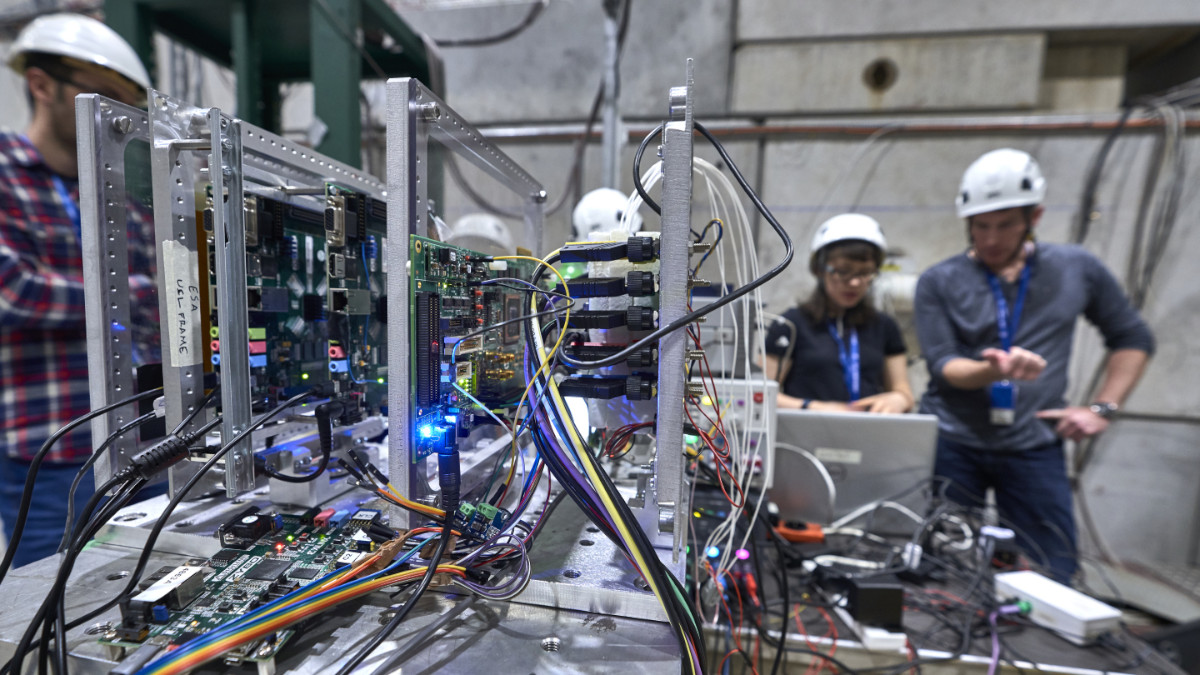
A system-on-chip tested for space applications by ESA at CERN Super Proton Synchrotron (SPS) North Area using a high energy lead-ion beam (Image: CERN, M. Brice).